
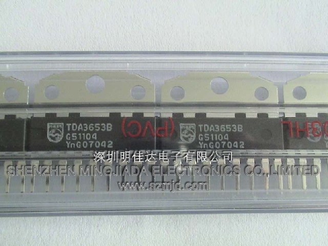
TDA3653 - Vertical deflection and guard circuit 90°
FUNCTIONAL DESCRIPTION
Output stage and protection circuit
Pin 5 is the output pin. The supply for the output stage is fed to pin 6 and the output stage ground is connected to pin 4.
The output transistors of the class-B output stage can each deliver 0.75 A maximum.
The maximum voltage for pin 5 and 6 is 60 V.
The output power transistors are protected such that their operation remains within the SOAR area. This is achieved by
the co-operation of the thermal protection circuit, the current-voltage detector, the short-circuit protection and the special
measures in the internal circuit layout.
Driver and switching circuit
Pin 1 is the input for the driver of the output stage. The signal at pin 1 is also applied via external resistors to pin 3 which
is the input of a switching circuit. When the flyback starts, this switching circuit rapidly turns off the lower output stage
and so limits the turn-off dissipation. It also allows a quick start of the flyback generator.
External connection of pin 1 to pin 3 allows for applications in which the pins are driven separately.
Flyback generator
During scan the capacitor connected between pins 6 and 8 is charged to a level which is dependent on the value of the
resistor at pin 8 (see Fig.1).
When the flyback starts and the voltage at the output pin (pin 5) exceeds the supply voltage, the flyback generator is
activated.
The supply voltage is then connected in series, via pin 8, with the voltage across the capacitor during the flyback period.
This implies that during scan the supply voltage can be reduced to the required scan voltage plus saturation voltage of
the output transistors.
The amplitude of the flyback voltage can be chosen by changing the value of the external resistor at pin 8.
It should be noted that the application is chosen such that the lowest voltage at pin 8 is > 2.5 V, during normal operation.
Guard circuit
When there is no deflection current and the flyback generator is not activated, the voltage at pin 8 reduces to less than
1.8 V. The guard circuit will then produce a DC voltage at pin 7, which can be used to blank the picture tube and thus
prevent screen damage.
Voltage stabilizer
The internal voltage stabilizer provides a stabilized supply of 6 V to drive the output stage, which prevents the drive
current of the output stage being affected by supply voltage variations.
由于客户采购批量与样品的价格不同,网上无法统一注明,请您把采购型号通过邮件或客服QQ:2850151585 发给我们,也可以拨打明佳达国内销售部电话:0755-83957301,由客服人员为您报价;有时元件厂商价格稍许变动,本公司未能及时调整,如您觉得售价稍高,请与我们说明并适当议价,感谢支持!
MJD is a corporation which engaged in agency electronic components. MJD Through seventeen years unrimitting efforts, aspire to provide our customers with world-leading products and service. Now already became a one of the most famous electronic components distributor in China.
-------------------------------------------------------------------------------------------------------------------------------------------------------------------------------------
PAYMENTS:
We support the following payment methods:
1. Paypal
2. Western Union
3. Bank Wire (TT)
4. MoneyGram
Shipping:
1. MJD needs about 3 BUSINESS DAY to handle the order after received payment. after receiving your payment. Otherwise, we will state it in the invoice in advance.
2. MJD can Ship via your shipping account (DHL / FEDEX / UPS / TNT or others) as your instruction. Or Ship via our shipping account (We have a very good relationship with DHL and FEDEX with very special freight).
3. Regarding the declared value on the package for customs clearance, we are pleased to follow
your wishes, just feel free to inform us when ordering.
4. Any import fees or charges are the buyer's responsibility.
REFUNDS & RETURN:
We offer a warranty on all items that we sold. Item will be tested before ship,it will be in good condition,if there are some problems with the item,feel free to contact us.Please Email us to notify a defective item. Unless otherwise specified, this item comes with 30 days warranty from the shipment date.
You must contact us before returning any product. All returns must be made within 30 days from this shipment date.Return must be in new condition(the SAME CONDITION as it was sent to you)
Because of wholesale price is different from sample price, our website can not state. Please send your required part number via email Sales@hkmjd.com or skype id mjdccm898 to us. As well as welcome you call us : 0755-83957301 We will send offer for you; Sometimes manufacturer's price is unstable, so we don't adjust price in time. if you feel price is a little high for you, just feel free to contact us for consultation. Thank you for your support !
| 型号 | 品牌 | 批号 | 封装 | 数量 | 备注 | 资料 |
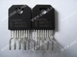
| TDA8359J | NXP | 13+RoHs | ZIP | 550250 | 100% 全新原装 (New and original) |
|
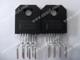
| TDA4863AJ | NXP | 13+RoHs | ZIP7 | 68000 | 100% 全新原装(Brand new) |
|
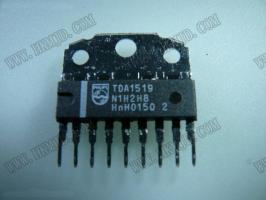
| TDA1519 | NXP | 13+ | ZIP-9 | 85780 | 原装进口现货Original |
|
| TDA1519C | NXP | 13+ | ZIP-9 | 6500 | 原装进口现货Original |
|
| TDA18250HN | NXP | 16+ | QFN | 85780 | 100%全新原装 New in stock |
|
| TDA18273HN | NXP | 14+RoHS | QFN | 7470 | 专业分销原装NXP Original |
|
| TDA19989AET | NXP | 13+ | BGA | 7740 | 100%全新原装 New in stock |
|
| TDA3683 | NXP | 13+ | ZIP | 4580 | 专业分销原装NXP Original |
|